Custom Search
|
|
  |
|
|
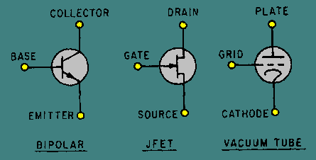
Field Effect Transistors Although it has brought about a revolution in the design of electronic equipment, the bipolar (PNP/NPN) transistor still has one very undesirable characteristic. The low input impedance associated with its base-emitter junction causes problems in matching impedances between interstage amplifiers. For years, scientists searched for a solution that would combine the high input impedance of the vacuum tube with the many other advantages of the transistor. The result of this research is the FIELD-EFFECT TRANSISTOR (FET). In contrast to the bipolar transistor, which uses bias current between base and emitter to control conductivity, the FET uses voltage to control an electrostatic field within the transistor. Because the FET is voltage-controlled, much like a vacuum tube, it is sometimes called the "solid-state vacuum tube." The elements of one type of FET, the junction type (JFET), are compared with the bipolar transistor and the vacuum tube in figure 3-44. As the figure shows, the JFET is a three-element device comparable to the other two. The "gate" element of the JFET corresponds very closely in operation to the base of the transistor and the grid of the vacuum tube. The "source" and "drain" elements of the JFET correspond to the emitter and collector of the transistor and to the cathode and plate of the vacuum tube. Figure 3-44. - Comparison of JFET, transistor, and vacuum tube symbols.
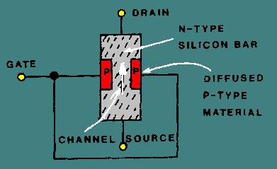
The construction of a JFET is shown in figure 3-45. A solid bar, made either of N-type or P-type material, forms the main body of the device. Diffused into each side of this bar are two deposits of material of the opposite type from the bar material, which form the "gate." The portion of the bar between the deposits of gate material is of a smaller cross section than the rest of the bar and forms a "channel" connecting the source and the drain. Figure 3-45 shows a bar of N-type material and a gate of P-type material. Because the material in the channel is N-type, the device is called an N-channel JFET. Figure 3-45. - JFET structure.
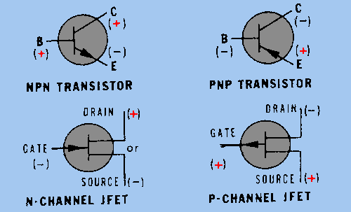
In a P-channel JFET, the channel is made of P-type material and the gate of N-type material. In figure 3-46, schematic symbols for the two types of JFET are compared with those of the NPN and PNP bipolar transistors. Like the bipolar transistor types, the two types of JFET differ only in the configuration of bias voltages required and in the direction of the arrow within the symbol. Just as it does in transistor symbols, the arrow in a JFET symbol always points towards the N-type material. Thus the symbol of the N-channel JFET shows the arrow pointing toward the drain/source channel, whereas the P-channel symbol shows the arrow pointing away from the drain/source channel toward the gate. Figure 3-46. - Symbols and bias voltages for transistors and JFET.
The key to FET operation is the effective cross-sectional area of the channel, which can be controlled by variations in the voltage applied to the gate. This is demonstrated in the figures which follow. Figure 3-47 shows how the JFET operates in a zero gate bias condition. Five volts are applied across the JFET so that current flows through the bar from source to drain, as indicated by the arrow. The gate terminal is tied to ground. This is a zero gate bias condition. In this condition, a typical bar represents a resistance of about 500 ohms. A milliammeter, connected in series with the drain lead and dc power, indicates the amount of current flow. With a drain supply (VDD) of 5 volts, the milliammeter gives a drain current (ID) reading of 10 milliamperes. The voltage and current subscript letters (VDD, ID) used for an FET correspond to the elements of the FET just as they do for the elements of transistors. Figure 3-47. - JFET operation with zero gate bias.
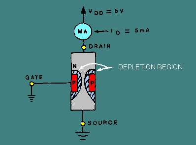
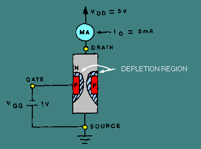
In figure 3-48, a small reverse-bias voltage is applied to the gate of the JFET. A gate-source voltage (VGG) of negative 1 volt applied to the P-type gate material causes the junction between the P- and N-type material to become reverse biased. Just as it did in the varactor diode, a reverse-bias condition causes a "depletion region" to form around the PN junction of the JFET. Because this region has a reduced number of current carriers, the effect of reverse biasing is to reduce the effective cross-sectional area of the "channel." This reduction in area increases the source-to-drain resistance of the device and decreases current flow. Figure 3-48. - JFET with reverse bias.
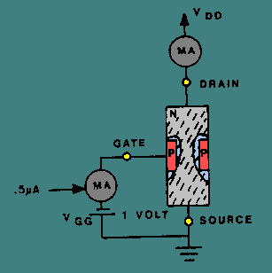
The application of a large enough negative voltage to the gate will cause the depletion region to become so large that conduction of current through the bar stops altogether. The voltage required to reduce drain current (ID) to zero is called "pinch-off" voltage and is comparable to "cut-off" voltage in a vacuum tube. In figure 3-48, the negative 1 volt applied, although not large enough to completely stop conduction, has caused the drain current to decrease markedly (from 10 milliamperes under zero gate bias conditions to 5 milliamperes). Calculation shows that the 1-volt gate bias has also increased the resistance of the JFET (from 500 ohms to 1 kilohm). In other words, a 1-volt change in gate voltage has doubled the resistance of the device and cut current flow in half. These measurements, however, show only that a JFET operates in a manner similar to a bipolar transistor, even though the two are constructed differently. As stated before, the main advantage of an FET is that its input impedance is significantly higher than that of a bipolar transistor. The higher input impedance of the JFET under reverse gate bias conditions can be seen by connecting a microammeter in series with the gate-source voltage (VGG), as shown in figure 3-49. Figure 3-49. - JFET input impedance.
With a VGG of 1 volt, the microammeter reads .5 microamps. Applying Ohm's law (1V .5mA) illustrates that this very small amount of current flow results in a very high input impedance (about 2 megohms). By contrast, a bipolar transistor in similar circumstances would require higher current flow (e.g., .1 to -1 mA), resulting in a much lower input impedance (about 1000 ohms or less). The higher input impedance of the JFET is possible because of the way reverse-bias gate voltage affects the cross-sectional area of the channel. The preceding example of JFET operation uses an N-channel JFET. However, a P-channel JFET operates on identical principles. The differences between the two types are shown in figure 3-50. |
 |
|
|
Integrated Publishing, Inc. - A (SDVOSB) Service Disabled Veteran Owned Small Business
|