Custom Search
|
|
  |
|
|
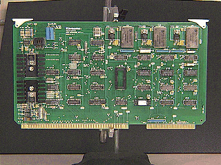
SOLID-STATE DEVICES Now would be a good time for you to review the first few pages of NEETS, Module 7, Introduction to Solid-State Devices and Power Supplies, as a refresher for solid-state devices. The transition from vacuum tubes to solid-state devices took place rapidly. As new types of transistors and diodes were created, they were adapted to circuits. The reductions in size, weight, and power use were impressive. Circuits that earlier weighed as much as 50 pounds were reduced in weight to just a few ounces by replacing bulky components with the much lighter solid-state devices. The earliest solid-state circuits still relied on point-to-point wiring which caused many of the disadvantages mentioned earlier. A metal chassis, similar to the type used with tubes, was required to provide physical support for the components. The solid-state chassis was still considerably smaller and lighter than the older, tube chassis. Still greater improvements in component mounting methods were yet to come. One of the most significant developments in circuit packaging has been the PRINTED CIRCUIT BOARD (pcb), as shown in figure 1-3. The pcb is usually an epoxy board on which the circuit leads have been added by the PHOTOETCHING process. This process is similar to photography in that copper-clad boards are exposed to controlled light in the desired circuit pattern and then etched to remove the unwanted copper. This process leaves copper strips (LANDS) that are used to connect the components. In general, printed circuit boards eliminate both the heavy, metal chassis and the point-to-point wiring. Figure 1-3. - Printed circuit board (pcb).
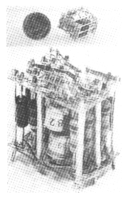
Although printed circuit boards represent a major improvement over tube technology, they are not without fault. For example, the number of components on each board is limited by the sizes and shapes of components. Also, while vacuum tubes are easily removed for testing or replacement, pcb components are soldered into place and are not as easily removed. Normally, each pcb contains a single circuit or a subassembly of a system. All printed circuit boards within the system are routinely interconnected through CABLING HARNESSES (groups of wiring or ribbons of wiring). You may be confronted with problems in faulty harness connections that affect system reliability. Such problems are often caused by wiring errors, because of the large numbers of wires in a harness, and by damage to those wires and connectors. Another mounting form that has been used to increase the number of components in a given space is the CORDWOOD MODULE, shown in figure 1-4. You can see that the components are placed perpendicular to the end plates. The components are packed very closely together, appearing to be stacked like cordwood for a fireplace. The end plates are usually small printed circuit boards, but may be insulators and solid wire, as shown in the figure. Cordwood modules may or may not be ENCAPSULATED (totally imbedded in solid material) but in either case they are difficult to repair. Figure 1-4. - Cordwood module.
Q.9 List the major advantages of printed circuit boards. |
 |
|
|
Integrated Publishing, Inc. - A (SDVOSB) Service Disabled Veteran Owned Small Business
|