Custom Search
|
|
  |
|
|
SUMMARY Now that we have completed this chapter, a short review of the more important points covered in the chapter will follow. You should be thoroughly familiar with these points before continuing on to chapter 2. The UNIVERSE consists of two main parts-matter and energy. MATTER is anything that occupies space and has weight. Rocks, water, and air are examples of matter. Matter may be found in any one of three states: solid, liquid and gaseous. It can also be composed of either an element or a combination of elements. An ELEMENT is a substance that cannot be reduced to a simpler form by chemical means. Iron, gold, silver, copper, and oxygen are all good examples of elements. A COMPOUND is a chemical combination of two or more elements. Water, table salt, ethyl alcohol, and ammonia are all examples of compounds. A MOLECULE is the smallest part of a compound that has all the characteristics of the compound. Each molecule contains some of the atoms of each of the elements forming the compound. The ATOM is the smallest particle into which an element can be broken down and still retain all its original properties. An atom is made up of electrons, protons, and neutrons. The number and arrangement of these particles determine the kind of element.
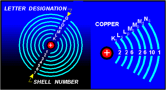
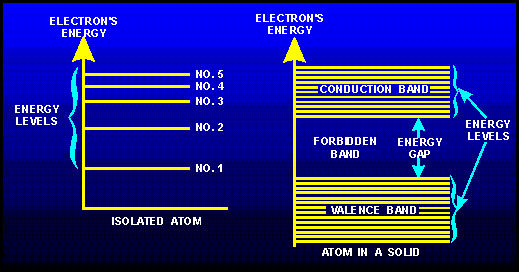
An ELECTRON carries a small negative charge of electricity. The PROTON carries a positive charge of electricity that is equal and opposite to the charge of the electron. However, the mass of the proton is approximately 1,837 times that of the electron. The NEUTRON is a neutral particle in that it has no electrical charge. The mass of the neutron is approximately equal to that of the proton. An ELECTRON'S ENERGY LEVEL is the amount of energy required by an electron to stay in orbit. Just by the electron's motion alone, it has kinetic energy. The electron's position in reference to the nucleus gives it potential energy. An energy balance keeps the electron in orbit and as it gains or loses energy, it assumes an orbit further from or closer to the center of the atom. SHELLS and SUBSHELLS are the orbits of the electrons in an atom. Each shell can contain a maximum number of electrons, which can be determined by the formula 2n2. Shells are lettered K through Q, starting with K, which is the closest to the nucleus. The shell can also be split into four subshells labeled s, p, d, and f, which can contain 2, 6, 10, and 14 electrons, respectively.
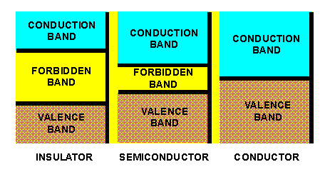
VALENCE is the ability of an atom to combine with other atoms. The valence of an atom is determined by the number of electrons in the atom's outermost shell. This shell is referred to as the VALENCE SHELL. The electrons in the outermost shell are called VALENCE ELECTRONS. IONIZATION is the process by which an atom loses or gains electrons. An atom that loses some of its electrons in the process becomes positively charged and is called a POSITIVE ION. An atom that has an excess number of electrons is negatively charged and is called a NEGATIVE ION. ENERGY BANDS are groups of energy levels that result from the close proximity of atoms in a solid. The three most important energy bands are the CONDUCTION BAND, FORBIDDEN BAND, and VALENCE BAND.
CONDUCTORS, SEMICONDUCTORS, and INSULATORS are categorized as such by using the energy band concept. It is the width of the forbidden band that determines whether a material is an insulator, a semiconductor, or a conductor. A CONDUCTOR has a very narrow forbidden band or none at all. A SEMICONDUCTOR has a medium width forbidden band. An INSULATOR has a wide forbidden band.
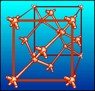
COVALENT BONDING is the sharing of valence electrons between two or more atoms. It is this bonding that holds the atoms together in an orderly structure called a CRYSTAL.
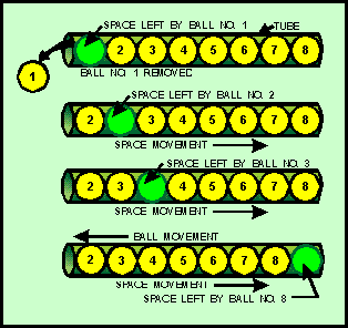
The CONDUCTION PROCESS in a SEMICONDUCTOR is accomplished by two different types of current flow: HOLE FLOW and ELECTRON FLOW. Hole flow is very similar to electron flow except that holes (positive charges) move toward a negative potential and in an opposite direction to that of the electrons. In an INTRINSIC semiconductor (one which does not contain any impurities), the number of holes always equals the number of conducting electrons.
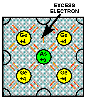
DOPING is the process by which small amounts of selected additives, called impurities, are added to semiconductors to increase their current flow. Semiconductors that undergo this treatment are referred to as EXTRINSIC SEMICONDUCTORS. An N-TYPE SEMICONDUCTOR is one that is doped with an N-TYPE or donor impurity (an impurity that easily loses its extra electron to the semiconductor causing it to have an excess number of free electrons). Since this type of semiconductor has a surplus of electrons, the electrons are considered the majority current carriers, while the holes are the minority current carriers.
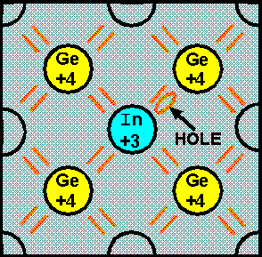
A P-TYPE SEMICONDUCTOR is one which is doped with a P-TYPE or acceptor impurity (an impurity that reduces the number of free electrons causing more holes). The holes in this type semiconductor are the majority current carriers since they are present in the greatest quantity while the electrons are the minority current carriers.
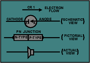
The SEMICONDUCTOR DIODE, also known as a PN JUNCTION DIODE, is a two-element semiconductor device that makes use of the rectifying properties of a PN junction to convert alternating current into direct current by permitting current flow in only one direction.
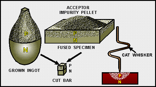
A PN JUNCTION CONSTRUCTION varies from one manufacturer to the next. Some of the more commonly used manufacturing techniques are: GROWN, ALLOY or FUSED-ALLOY , DIFFUSED, and POINT-CONTACT.
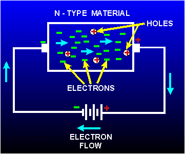
CURRENT FLOW in an N-TYPE MATERIAL is similar to conduction in a copper wire. That is, with voltage applied across the material, electrons will move through the crystal toward the positive terminal just like current flows in a copper wire.
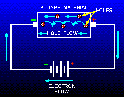
CURRENT FLOW in a P-TYPE MATERIAL is by positive holes, instead of negative electrons. Unlike the electron, the hole moves from the positive terminal of the P material to the negative terminal.
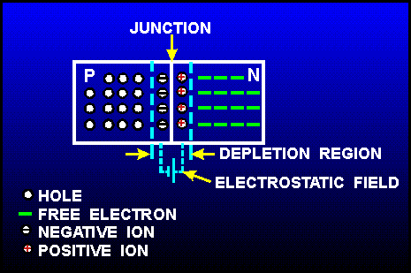
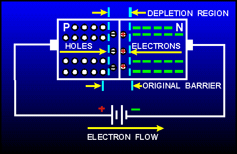
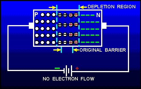
JUNCTION BARRIER is an electrostatic field that has been created by the joining of a section of N material with a section of P material. Since holes and electrons must overcome this field to cross the junction, the electrostatic field is commonly called a BARRIER. Because there is a lack or depletion of free electrons and holes in the area around the barrier, this area has become known as the DEPLETION REGION.
FORWARD BIAS is an external voltage that is applied to a PN junction to reduce its barrier and, therefore, aid current flow through the junction. To accomplish this function, the external voltage is connected so that it opposes the electrostatic field of the junction.
REVERSE BIAS is an external voltage that is connected across a PN junction so that its voltage aids the junction and, thereby, offers a high resistance to the current flow through the junction.
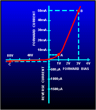
The PN JUNCTION has a unique ability to offer very little resistance to current flow in the forward-bias direction, but maximum resistance to current flow when reverse biased. For this reason, the PN junction is commonly used as a diode to convert ac to dc.
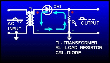
The PN JUNCTION'S APPLICATION expands many different areas-from a simple voltage protection device to an amplifying diode. Two of the most commonly used applications for the PN junction are the SIGNAL DIODE (mixing, detecting, and switching signals) and the RECTIFYING DIODE (converting ac to dc).
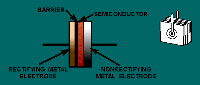
The METALLIC RECTIFIER or dry-disc rectifier is a metal-to-semiconductor device that acts just like a diode in that it permits current to flow more readily in one direction than the other. Metallic rectifiers are used in many applications where a relatively large amount of power is required.
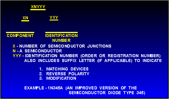
DIODE CHARACTERISTICS is the information supplied by manufacturers on different types of diodes, either in their manuals or on specification sheets. DIODE RATINGS are the limiting value of operating conditions of a diode. Operation of the diode outside of its operating limits could damage the diode. Diodes are generally rated for: MAXIMUM AVERAGE FORWARD CURRENT, PEAK RECURRENT FORWARD CURRENT , MAXIMUM SURGE CURRENT, and PEAK REVERSE VOLTAGE. The SEMICONDUCTOR IDENTIFICATION SYSTEM is an alphanumerical code used to distinguish one semiconductor from another. It is used for diodes, transistors, and many other special semiconductor devices.
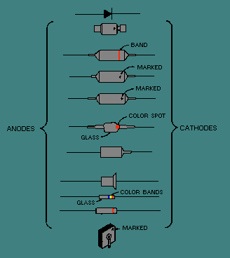
DIODE MARKINGS are letters and symbols placed on the diode by manufacturers to distinguish one end of the diode from the other. In some cases, an unusual shape or the addition of color code bands is used to distinguish the cathode from the anode.
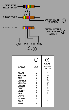
The STANDARD DIODE COLOR CODE SYSTEM serves two purposes when it is used: (1) it identifies the cathode end of the diode, and (2) it also serves to identify the diode by number.
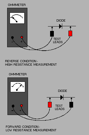
DIODE MAINTENANCE is the procedures or methods used to keep a diode in good operating condition. To prevent diode damage, you should observe standard diode safety precautions and ensure that diodes are not subjected to heat, current overloads, and excessively high operating voltages. TESTING A DIODE can be accomplished by using an ohmmeter, the substitution method, or a dynamic diode tester. The most convenient and quickest way of testing a diode is with an ohmmeter.
|
 |