Custom Search
|
|
  |
|
|
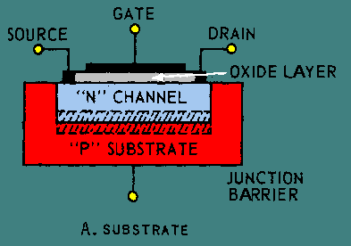
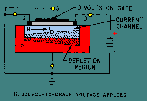
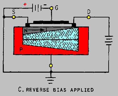
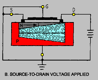
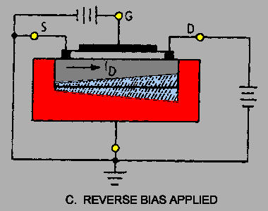
Figure 3-54A. - Effects of bias on N-channel depletion MOSFET.
Figure 3-54B. - Effects of bias on N-channel depletion MOSFET.
Figure 3-54C. - Effects of bias on N-channel depletion MOSFET.
Figure 3-55 (view A, view B, and view C) illustrates the effect of forward bias on an enhancement mode N-channel MOSFET. In this case, a positive voltage applied to the gate increases the width of the current channel and the amount of drain current (ID). Figure 3-55A. - Effects of bias on N-channel enhancement MOSFET.
Figure 3-55B. - Effects of bias on N-channel enhancement MOSFET.
Figure 3-55C. - Effects of bias on N-channel enhancement MOSFET.
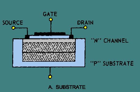
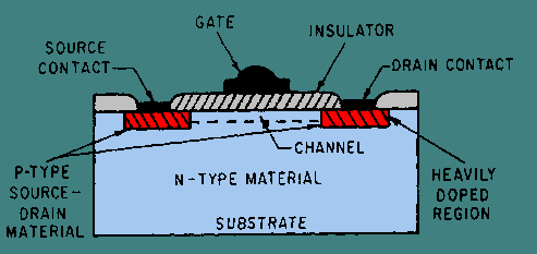
Another type of MOSFET is the induced-channel type MOSFET. Unlike the MOSFETs discussed so far, the induced-channel type has no actual channel between the source and the drain. The induced channel MOSFET is constructed by making the channel of the same type material as the substrate, or the opposite of the source and the drain material. As shown in figure 3-56, the source and the drain are of P-type material, and the channel and the substrate are of N-type material. Figure 3-56. - Induced channel MOSFET construction.
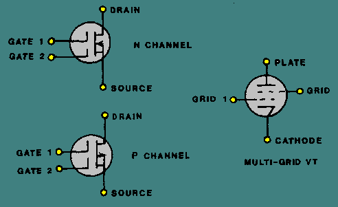
The induced-channel MOSFET is caused to conduct from source to drain by the electric field that is created when a voltage is applied to the gate. For example, assume that a negative voltage is applied to the MOSFET in figure 3-56. The effect of the negative voltage modifies the conditions in the substrate material. As the gate builds a negative charge, free electrons are repelled, forming a depletion region. Once a certain level of depletion has occurred (determined by the composition of the substrate material), any additional gate bias attracts positive holes to the surface of the substrate. When enough holes have accumulated at the surface channel area, the channel changes from an N-type material to a P-type material, since it now has more positive carriers than negative carriers. At this point the channel is considered to be to inverted, and the two P-type regions at the source and the drain are now connected by a P-type inversion layer or channel. As with the MOSFET, the gate signal determines the amount of current flow through the channel as long as the source and drain voltages remain constant. When the gate voltage is at zero, essentially no current flows since a gate voltage is required to form a channel. The MOSFETs discussed up to this point have been single-gate MOSFETs. Another type of MOSFET, the dual-gate type, is shown in figure 3-57. As the figure shows, the gates in a dual-gate MOSFET can be compared to the grids in a multi-grid vacuum tube. Because the substrate has been connected directly to the source terminal, the dual-gate MOSFET still has only four leads: one each for source and drain, and two for the gates. Either gate can control conduction independently, making this type of MOSFET a truly versatile device. Figure 3-57. - Dual-gate MOSFET.
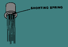
One problem with both the single- and dual-gate MOSFETs is that the oxide layer between gate and channel can be destroyed very easily by ordinary static electricity. Replacement MOSFETs come packaged with their leads shorted together by a special wire loop or spring to avoid accidental damage. The rule to remember with these shorting springs is that they must not be removed until after the MOSFET has been soldered or plugged into a circuit. One such spring is shown in figure 3-58. Figure 3-58. - MOSFET shorting spring.
Q.30 What is one of the primary advantages of the FET when compared to the bipolar
transistor? |
 
|
|
|
Integrated Publishing, Inc. - A (SDVOSB) Service Disabled Veteran Owned Small Business
|