Custom Search
|
|
  |
|
|
SUMMARY This chapter introduced you to a representative selection of solid-state devices that have special properties. The basic operating principles of the devices discussed in this chapter are summarized in the following paragraphs for you to use as a review and a future reference. The ZENER DIODE is a PN junction that is designed to operate in the reverse-bias breakdown mode. When the applied voltage reaches the breakdown point, the Zener diode, for all practical purposes, becomes a short circuit. The reverse bias and breakdown mode of operation cause the Zener diode to conduct with (in the direction of) the arrow in the symbol as shown.
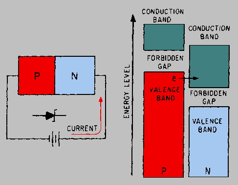
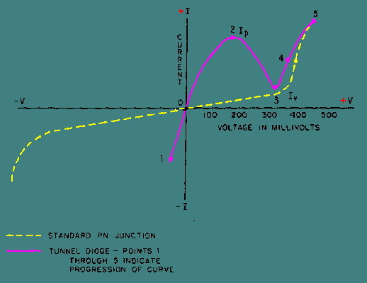
Two theories are used to explain the breakdown action of Zener diodes. The ZENER EFFECT explains the breakdown of diodes below 5 volts. The heavy doping used in these diodes allows the valence band of one material to overlap the energy level of the conduction band of the other material. This situation allows electrons to tunnel across the PN junction at the point where the two energy bands overlap. Zener diodes that operate above 5 volts are explained by the AVALANCHE EFFECT in which free electrons colliding with bound electrons cause an ever-increasing number of free current carriers in a multiplying action. The Zener diode is used primarily as a voltage regulator in electronic circuits. The TUNNEL DIODE is a heavily doped PN junction that exhibits negative resistance over part of its range of operation, as can be seen in the curve in the illustration. The heavy doping causes the tunnel diode to have a very narrow depletion region and also causes the valence band of one of the semiconductor materials to overlap the energy level of the conduction band of the other semiconductor material. At the energy overlap point, electrons can cross from the valence band of one material to the conduction band of the other material without acquiring any additional energy. This action is called tunneling. Tunnel diodes are used as amplifiers, oscillators, and high-speed switching devices.
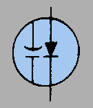
The VARACTOR is a diode that exhibits the characteristics of a variable capacitor. The depletion region at the PN junction acts as the dielectric of a capacitor and is caused to expand and contract by the voltage applied to the diode. This action increases and decreases the capacitance. The schematic symbol for the varactor is shown below. Varactors are used in tuning circuits and can be used as high-frequency amplifiers.
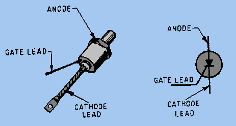
The SILICON CONTROLLED RECTIFIER (SCR) is a four-element, solid-state device that combines characteristics of both diodes and transistors. The symbol for the SCR is shown below. A signal must be applied to the gate to cause the SCR to conduct. When the proper gate signal is applied, the SCR conducts or "fires" until the bias potential across the device drops below the minimum required to sustain current flow. Removal of the gate signal does not shut off the SCR. In fact, the gate signal is often a very narrow voltage pulse or trigger. The SCR is ideal for use in situations where a small, low-power gate can be used to turn on larger currents, such as those found in rectifier and switching circuits. SCRs are used extensively in power supply circuits as rectifiers.
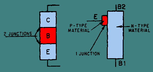
OPTOELECTRONIC DEVICES are of two basic types: light producers or light users. The LED is the most widely used light-producing device. When the LED is forward biased it emits energy in the form of light. LEDs are used in several configurations as digital equipment readout displays. The PHOTODIODE, the PHOTOTRANSISTOR, and the PHOTOCELL are all devices that use light to modify conduction through them. The SOLAR CELL uses light to produce voltage. The UNIJUNCTION TRANSISTOR (UJT) is a three-terminal, solid-state device with only one PN junction. The block diagram below shows the difference in construction between normal transistors and the UJT. The area between base 1 and base 2 of the UJT acts as a variable resister. The emitter of the UJT acts as the wiper arm. The sequential rise in voltage between the bases is called a voltage gradient. The UJT conducts when the emitter is more positive than the voltage gradient at the emitter/base contact point. There are many variations of the UJT which are used in switching circuits, oscillators, and wave-shaping circuits.
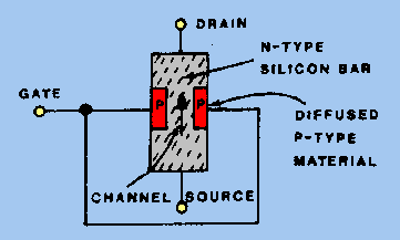
The FIELD-EFFECT TRANSISTOR combines the high input impedance of the vacuum tube with all the other advantages of the transistor. The elements of the FET are the gate, source, and drain, which are comparable to the base, emitter, and collector of a standard transistor. The JFET or "junction FET" is made of a solid bar of either P- or N-semiconductor material, and the gate is made of the opposite type material, as illustrated below. The FET is called P-channel or N-channel depending upon the type of material used to make the bar between the source and drain. Voltage applied to the gate controls the width of the channel and consequently controls the current flow from the source to the drain. The JFET is normally operated with reverse bias that controls the channel width by increasing or decreasing the depletion region.
The MOSFET is an FET that has even higher input impedances than the JFET because the gate of the MOSFET is completely insulated from the rest of the device. The MOSFET operates in either the depletion mode or the forward-bias enhancement mode and can be either N-channel or P-channel. The induced-channel and the dual-gate MOSFETs are variations of the basic MOSFET. |
 |
|
|
Integrated Publishing, Inc. - A (SDVOSB) Service Disabled Veteran Owned Small Business
|